
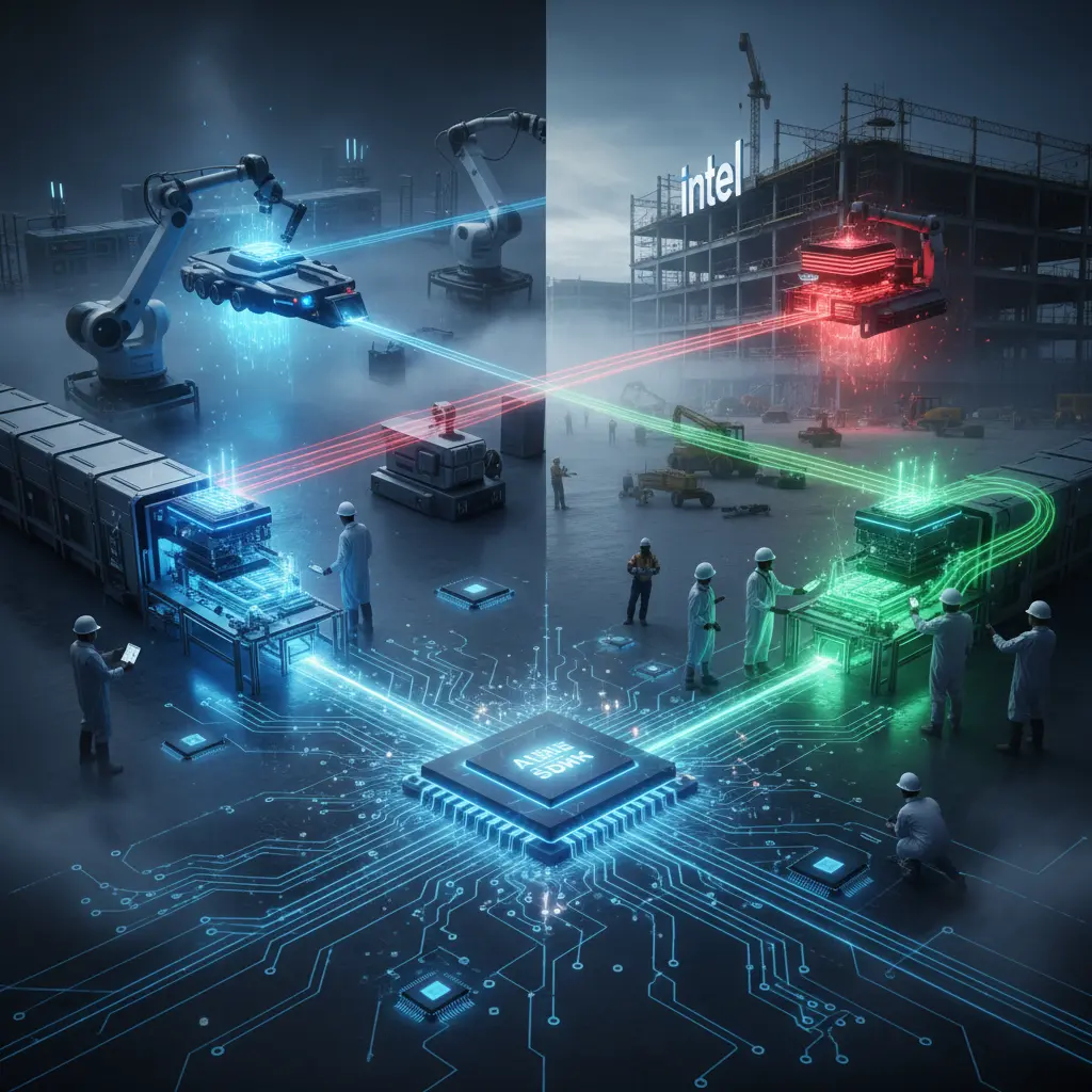
There’s a quiet arms race happening in South Korea and the United States right now, and it’s not about who can make chips faster — it’s about who can stack them better. Samsung is building out a massive new production line for a bonding technique that could reshape how memory chips are made. SK Hynix is hiring engineers in California to co-design an entirely new category of memory. And Intel, still trying to get its long-delayed Ohio megafab off the ground, is quietly talking to that same SK Hynix about a partnership. Three different moves, one shared driver: the AI boom has made memory the bottleneck, and nobody wants to be the company that falls behind.
Samsung Chip Technology Bets Big on Hybrid Bonding
Samsung Electronics is preparing to build a production-scale line at its Pyeongtaek campus equipped with roughly 50 die-to-wafer hybrid bonding tools, aimed squarely at next-generation high-bandwidth memory and advanced logic chips. Unlike the microbump-based methods chipmakers have relied on for years, hybrid bonding connects copper and dielectric materials directly, shortening the distance between stacked chips and cutting down on wasted space and heat. Samsung has reportedly picked Dutch equipment maker BE Semiconductor Industries as its preferred supplier, with equipment installation expected to begin toward the end of this year.
This is more than an incremental upgrade in Samsung chip technology — it’s a bet on where the whole industry is headed. Samsung showcased the underlying hybrid copper bonding approach at NVIDIA’s GTC event earlier this year, claiming it can support HBM stacks of 16 layers or more while cutting thermal resistance by over 20% compared to older thermal compression methods. The company is also working toward a next-generation “3D Cube-H” packaging architecture that would let it swap the standard HBM base die for a customer-specific logic die — effectively turning memory into something that can be tailored chip by chip for individual AI customers. Industry watchers note full-scale mass production may not arrive until closer to 2029 or 2030, but the groundwork being laid now shows how seriously Samsung is taking the shift.
HBM Memory Chips Move Beyond the Data Center
SK Hynix, meanwhile, is making its own next move — and it’s a telling one. The company has long led the HBM memory chips market that powers AI training clusters, but it’s now posting job listings through its San Jose subsidiary for engineers to co-design “3D Stacked DRAM-on-Logic” chips directly with U.S. clients. That’s a different battlefield entirely: rather than server racks, this technology targets on-device AI, vertically stacking DRAM on top of logic chips to break through the bandwidth and power limits of traditional smartphone chip packaging. Industry watchers have pointed to potential clients like Apple and Qualcomm, both of which have been pushing harder into on-device AI features.
It’s a sign that the competition between Samsung and SK Hynix isn’t just about who can pack more layers into a server-bound HBM stack — it’s spreading into every device category where AI workloads are starting to show up. SK Hynix has also been deepening its collaboration with NVIDIA on next-generation memory for AI factories, and recently became a founding partner of Applied Materials’ $5 billion Silicon Valley research center, where engineers from both companies will work side-by-side on future DRAM and HBM materials.
SK Hynix Intel Partnership Talk Adds a New Twist
Then there’s Intel, which has spent years trying to get its $28 billion Ohio semiconductor campus — its first new US fab in four decades — off the ground, only to push the opening date back repeatedly, most recently to 2030. According to recent reporting, Intel is now looking for a partner to help operate the Ohio site rather than sell it outright, and SK Hynix is among the companies being evaluated. SK Hynix has publicly denied any plan to acquire the facility, but people familiar with the discussions describe early-stage talks about a joint operating arrangement instead.
A SK Hynix Intel partnership on Ohio would echo the kind of capital-sharing deal Intel already has with Brookfield on its Arizona campus, where Intel retains majority ownership while an outside partner helps fund the buildout. For SK Hynix, which is already expanding memory capacity in Yongin, Cheongju, and Indiana, another US foothold would help it keep pace with a memory market that SK Group’s own chairman has said needs still more capacity. For Intel, it would offer a way to accelerate a project that’s badly needed a jolt of momentum — and possibly curry favor with a US government that now holds a strategic stake in the company.
Semiconductor Innovation Driven by One Thing: AI
Strip away the individual deals and a single thread runs through all of it. This is semiconductor innovation being reshaped almost entirely by AI demand. Training ever-larger models and running them efficiently on everything from data center GPUs to phones requires memory that can move data faster, sit closer to the processor, and run cooler while doing it. Hybrid bonding, 3D stacked DRAM-on-logic, and new fab partnerships are all different answers to the same underlying question — and for now, none of the major players seem willing to bet on just one approach.
What’s clear is that the chip manufacturing news cycle isn’t slowing down anytime soon. Samsung, SK Hynix, and Intel are each making moves that will take years to fully play out, but the direction is unmistakable: memory itself has become the frontier of the AI race, not just an accessory to it.